Molycop has invested in a state-of-the-art Scanning Electron Microscope (SEM) in Chile, giving customers faster problem-solving, deeper insights into material performance and solutions that extend equipment life and improve operational efficiency.
Key Facts
- The SEM enables rapid and precise diagnosis of wear issues, helping customers minimise downtime.
- High-resolution imaging and elemental analysis support smarter recommendations for grinding media and process optimisation.
- Investment in the SEM connects local expertise in Chile with Molycop’s global research network, ensuring world-class support for mining operations worldwide.
Towards that end, Molycop has deployed a TESCAN Vega LMS Scanning Electron Microscope (SEM) at its Chile Wear Research Lab.
 A key instrument in advanced research
In the field of microscopy and microanalysis, the SEM is considered an essential tool. It’s a cornerstone of advanced research and development in materials, metallurgical, mechanical and manufacturing engineering. Equipped with SE (Secondary Electron), BSE (Backscattered Electron), and EDS (Energy-Dispersive X-ray Spectroscopy) detectors, the SEM allows for:
- high-resolution imaging of microstructures and wear surfaces
- elemental analysis to identify material composition at the smallest scales
- advanced investigations into wear mechanisms, material performance and failure modes.
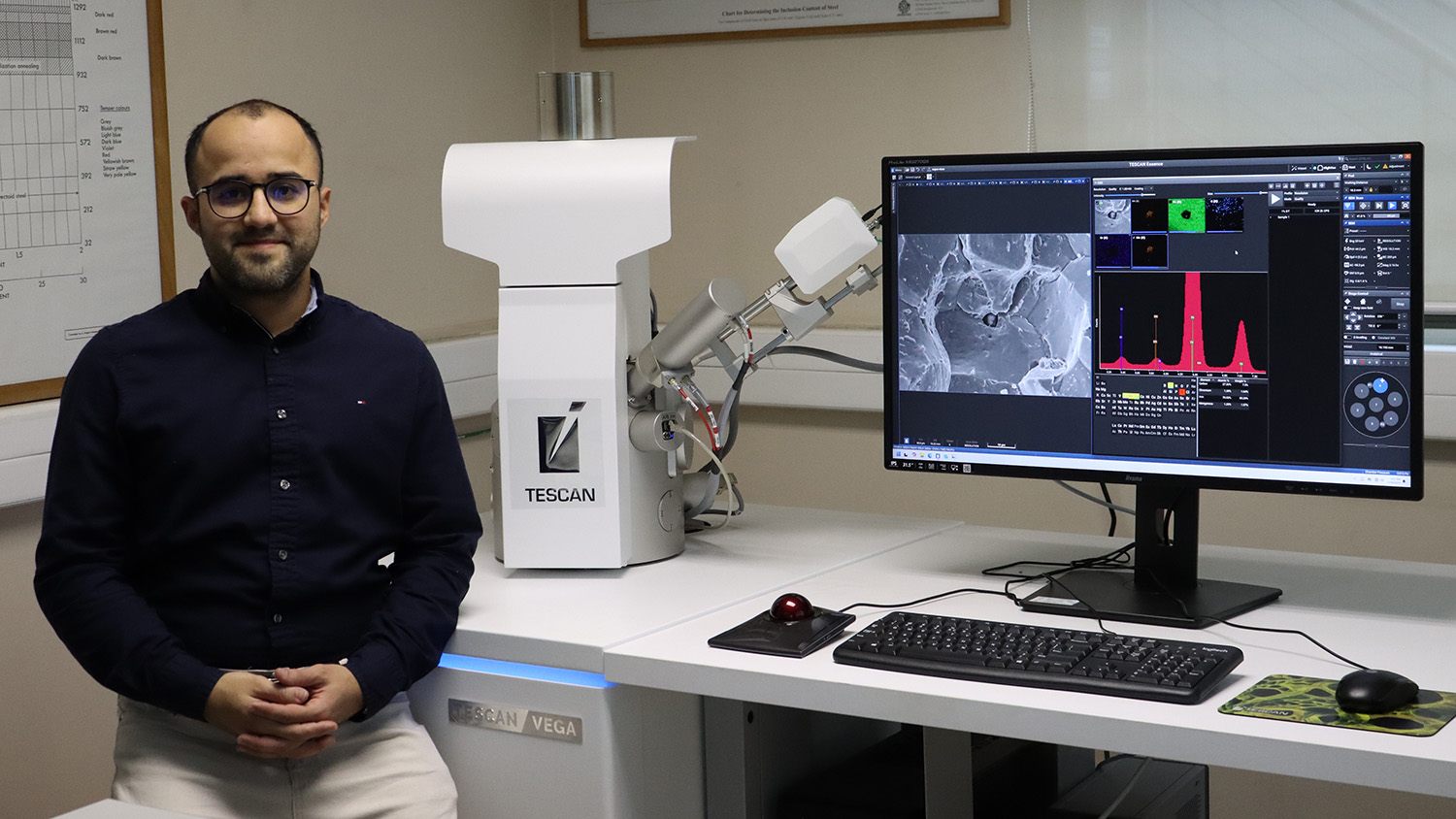
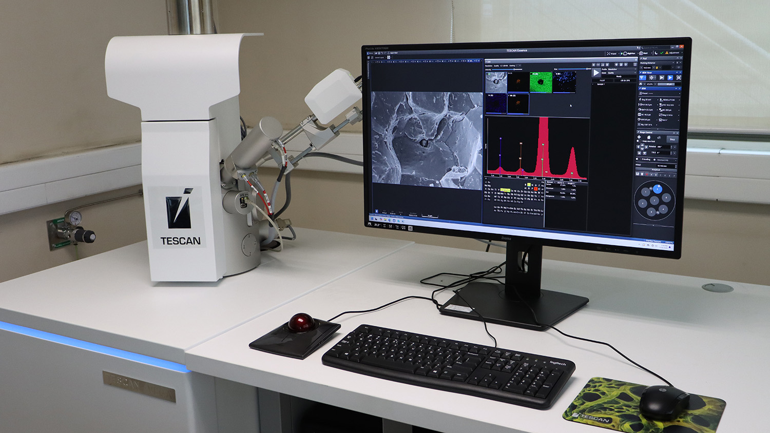 The TESCAN Vega LMS Scanning Electron Microscope (SEM) at Molycop's Chile Wear Research Lab.
Benefits for Molycop customers
The value of this investment lies in the practical advantages it offers Molycop’s customers:
- Faster, more accurate problem-solving – When a component shows signs of unexpected wear, the root cause can be diagnosed quickly.
- Optimised performance – Insights into microstructures and wear surfaces allow Molycop to recommend more effective grinding media and process strategies.
- Confidence in innovation – Molycop’s product development and technical support are backed by rigorous science and data.